
 Member login
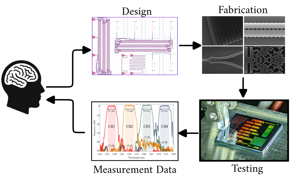
Interested in having your device fabricated and tested?
We are offering a free fabrication and test service, openEBL, for a small design area of 605 µm x 410 µm, to our international family of designers who are familiar with our EBeam process. The purpose is to allow people who have taken our courses or workshops to obtain fabrication & testing. We typically perform our fabrication/test runs 3 times per year.
The openEBL project is a SiEPICfab activity enabled by the contribution of its members. Design tools used are provided by free, open-source tools such as SiEPIC EPDA (SiEPIC-Tools and SiEPIC EBeam PDK) as well as Luceda (ipkiss) and gdsfactory. Fabrication is provided by Applied Nanotools and/or SiEPICfab internal fabrication process. Measurements are done by SiEPICfab using Maple Leaf Photonics measurement probe stations. Test and measurement instruments by Keysight Technologies.
Fabrication process
- 100keV Electron Beam Lithography at Applied Nanotools Inc and/or SiEPICfab internal process.
- 220 nm SOI with passivation oxide with both Passive-only process as well as passives+heaters with a single etch for active runs.
- Layers: 1 = silicon, 10 = text label for automated measurements; 99 = floorplan with a design area of: 605 µm x 410 µm.
Process Design Kit
- Open-source SiEPIC EDA can be used to design, simulate, and verify the devices using SiEPIC-Tools (EDA back-end), SiEPIC EBeam PDK (EBeam PDK add-on) with the free layout viewer, KLayout.
- Tutorials:
- SiEPIC EBeam PDK contains libraries of validated essential building blocks as well as libraries with lower-maturity devices (beta).
- Other PDKs are kindly provided by Luceda and gdsfactory. Any GDS that passes the DRC and verification checks can be submitted, irrespective of the EDA tool used.
- Please report any issues about the EDA or PDK in the repository’s ‘issues’ tab.
Design Submission
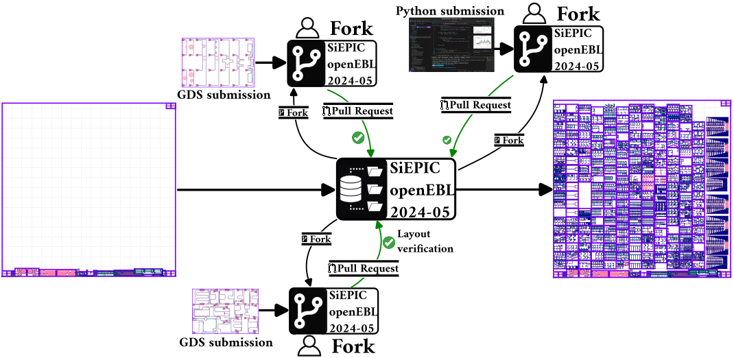
- Submission is done via GitHub using an automated merging and verification flow. (tutorial can be found on the submission repository’s homepage, video tutorial)
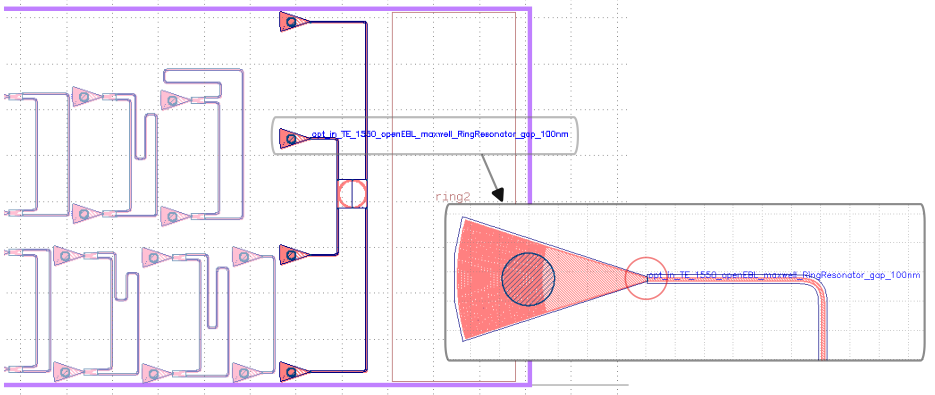
- Ensure that your designs contain the appropriate measurement labels format and location. Devices that do not contain measurement labels will not be measured.
- Measurement labels format:
- opt_in_[pol]_[wavelength]_openEBL_[yourname]_[deviceID]
- [pol] being the polarization (TE or TM)
- [wavelength] being the wavelength band of your device (1550 or 1310)
- [yourname] A unique username for you to identify your data
- [deviceID] being the device identifier, you can further underscores there as well.
- Do not use any illegal characters “, # < > $ % ^, etc.”. Underscores are okay.
- Example: opt_in_TE_1550_openEBL_maxwell_RingResonator_gap_100nm
- [pol] = TE
- [wavelength] = 1550
- [yourname] = maxwell
- [deviceID] = RingResonator_gap_100nm
- Measurement labels placement:
- Place the label near the tip of the input grating coupler. Grating couplers above and below the input will be measured by the detector)
- Must be placed on the text (10/0) layer.
For successful measurements, it is recommended to maximize the transmitted power from the source to one of either grating coupler above or below the input grating coupler.
For automated electro-optical measurements, please create your test routines using the SiEPIC Test Creator tool:
https://github.com/SiEPIC/SiEPIC_testcreator
Tape-out schedule
| Run ID | Design Due Date | Submission |
| openEBL-24-02 | 2024/2/10 | openEBL-2024-02 |
| openEBL-24-02-Heaters | 2024/2/10 | openEBL-2024-02-Heaters |
| openEBL-24-05 | 2024/5/18 | openEBL-2024-05 |
| openEBL-24-07-Heaters | 2024/5/18 | openEBL-2024-07-Heaters |
| openEBL-24-10 | 2024/10/12 | openEBL-2024-10 |
| openEBL-25-02 | 2025/2/15 | Not yet open. |
| openEBL-25-05 | 2025/5/17 | Not yet open. |
| openEBL-25-10 | 2025/10/11 | Not yet open. |
Please submit your inquiries about the submission process and tape-out in the issues tab of the submission repository.
Measurement results
- A link to the measurement results will be made available on the homepage of the submission repository as soon as they’re available (typically 4-6 weeks after tape-out date).
- Historical data from the past 1-2 years are available here. Older data for openEBL runs (2017-2023) can be made available upon reasonable request.
- Historical process control is summarized in the live PCM spreadsheet.
FAQs:
When will measurements be made available?
- Typically, 4-6 weeks after the tape-out date.
How mature is the PDK?
- The SiEPIC EBeam PDK is an open-source PDK that has been developed over many years. The PDK includes many well-validated essential building blocks in the “mature” library as well as less-validated components and complex PCells/devices in the “Beta” library. Many PCells are also provided. We look forward to your contribution!
What is the minimum feature size and spacing of silicon?
- 70 nm for both. A DRC file is provided in the SiEPIC EBeam PDK that can be used to execute DRC in KLayout.
My design is not being uploaded to the submission repository.
- Ensure the layout Verification is passing for your submitted design. Please submit your inquiry to the “Issues” tab in the repository page.
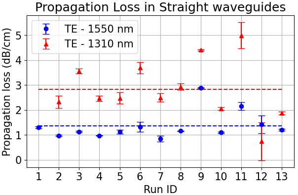
What is the typical waveguide propagation loss?
- Below are characterized waveguides from the past 13 measurement runs.
I cannot find my device in the measurement results and/or the device measurements directory is empty.
- If you can’t find the measurement directory for your device, ensure your device had the measurement labels in the proper format and placement.
- If the measurement directory is empty, that indicates that the automated measurement for your device has failed to measure any significant power above the measurement limit (noise and scattering).
What is the measurement wavelength range and conditions?
- Measurements are performed at 25C. The measurement wavelength range will depend on the instruments used at the time of measurement, typically <1500 nm to >1580 nm for C-band and (<1270 nm to >1330 nm) for O-band. Refer to the metadata of the historical measurement data files to obtain an estimate of the remaining measurement conditions.
Community
- Join the SiEPIC LinkedIn group to keep up on the latest news and events.
- Join the SiEPIC newsletter to stay up to date on upcoming runs and measurement results.
- Discover SiEPIC open-source projects: https://github.com/SiEPIC
Get involved with SiEPICfab.