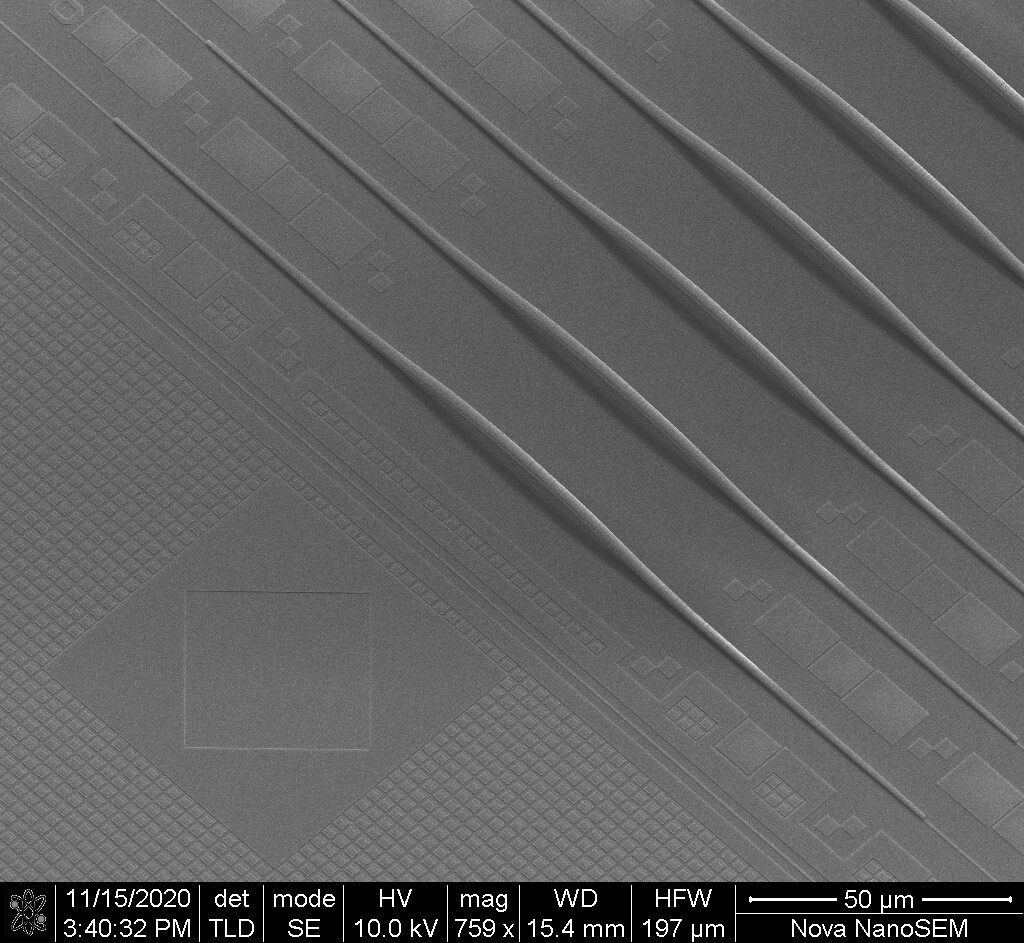
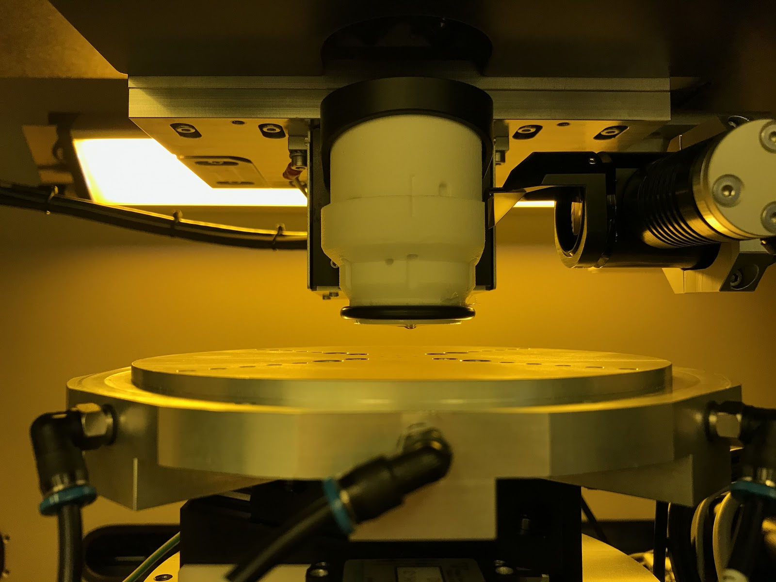
The companies involved span the entire lifecycle of silicon photonic chip research, design, fabrication, testing and application and implements both shared results and a confidential proprietary model that allows for streamlined prototyping of cutting edge circuit designs.
companies
universities
people
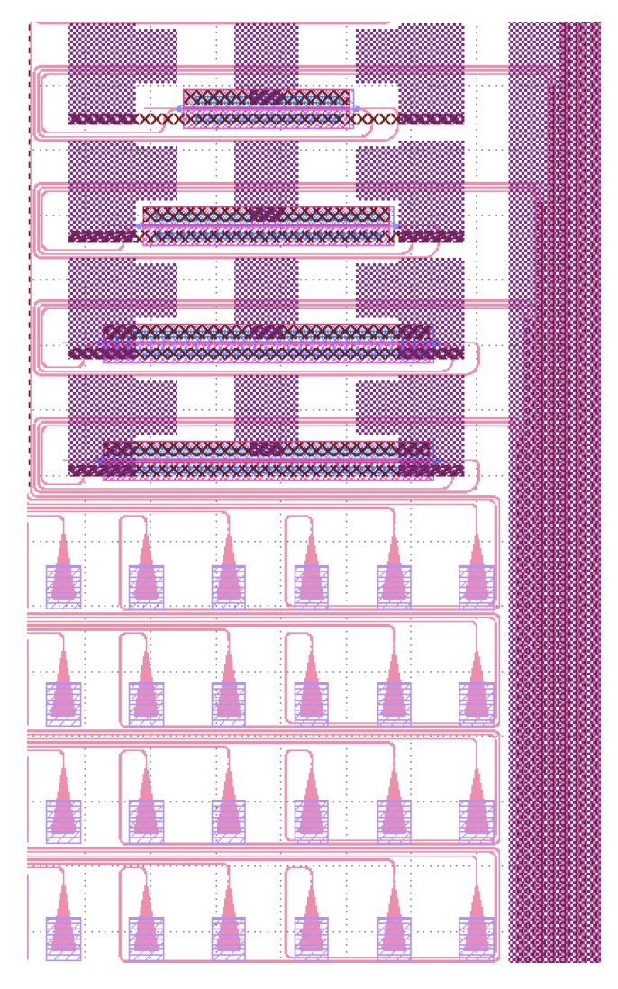
High performance photonic simulation software from ANSYS / Lumerical, and a complete design framework for photonic integrated circuits from Luceda Photonics
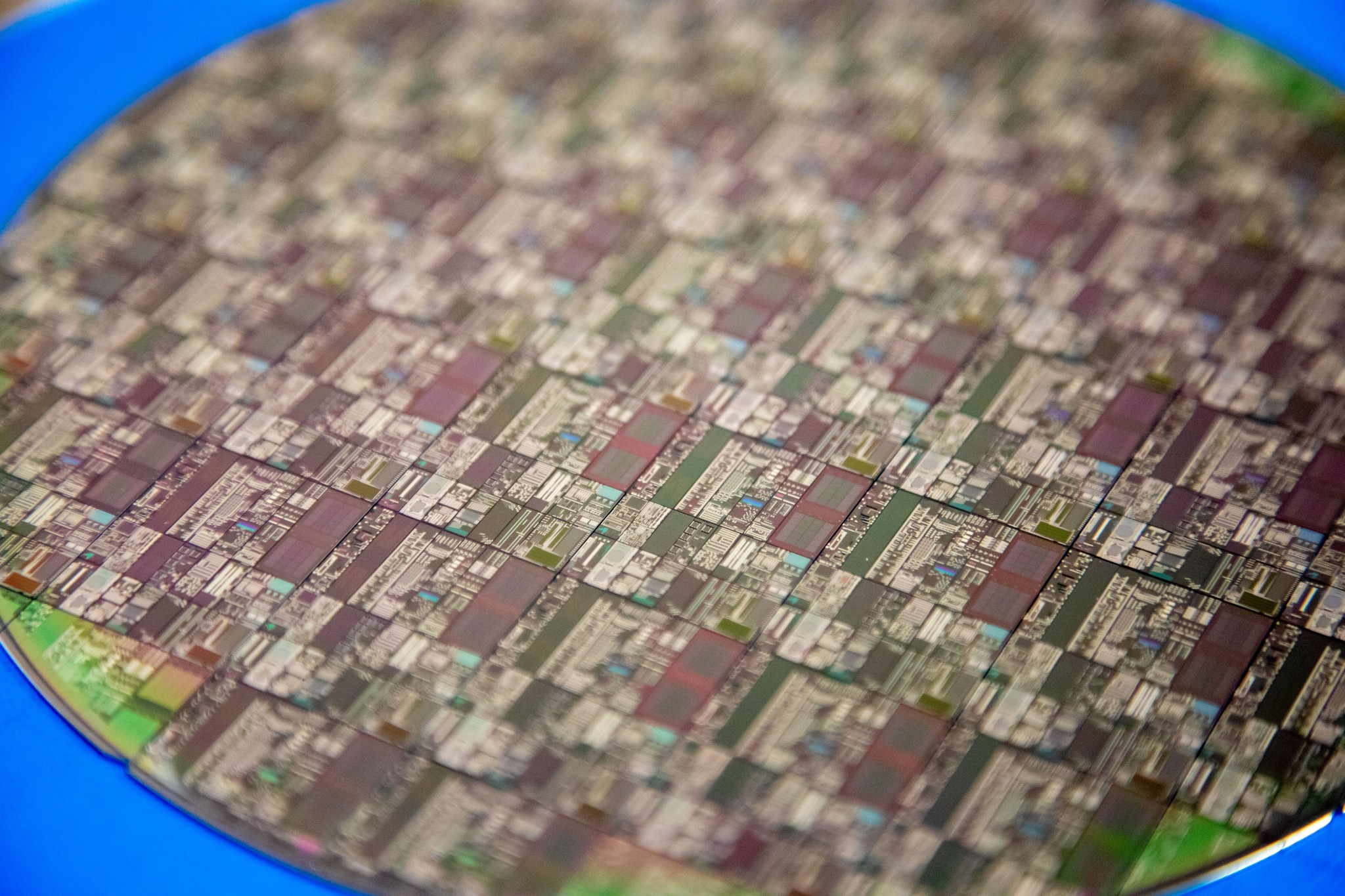
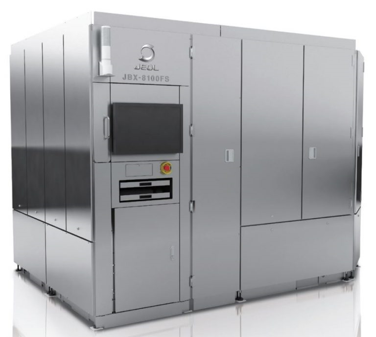
Fabrication and prototyping with 200mm compatible processes at UBC Nanofab and through translational partner Applied Nanotools. Nanofab facilities include a state-of-the-art 100kV JEOL 8100FS Electron Beam Lithography system.
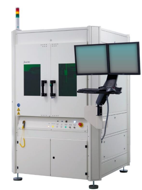
Sonata1000 Photonic Wirebond tool from Vanguard Automation delivers bleeding edge scalable optical packaging solution with low loss coupling to a wide variety of devices
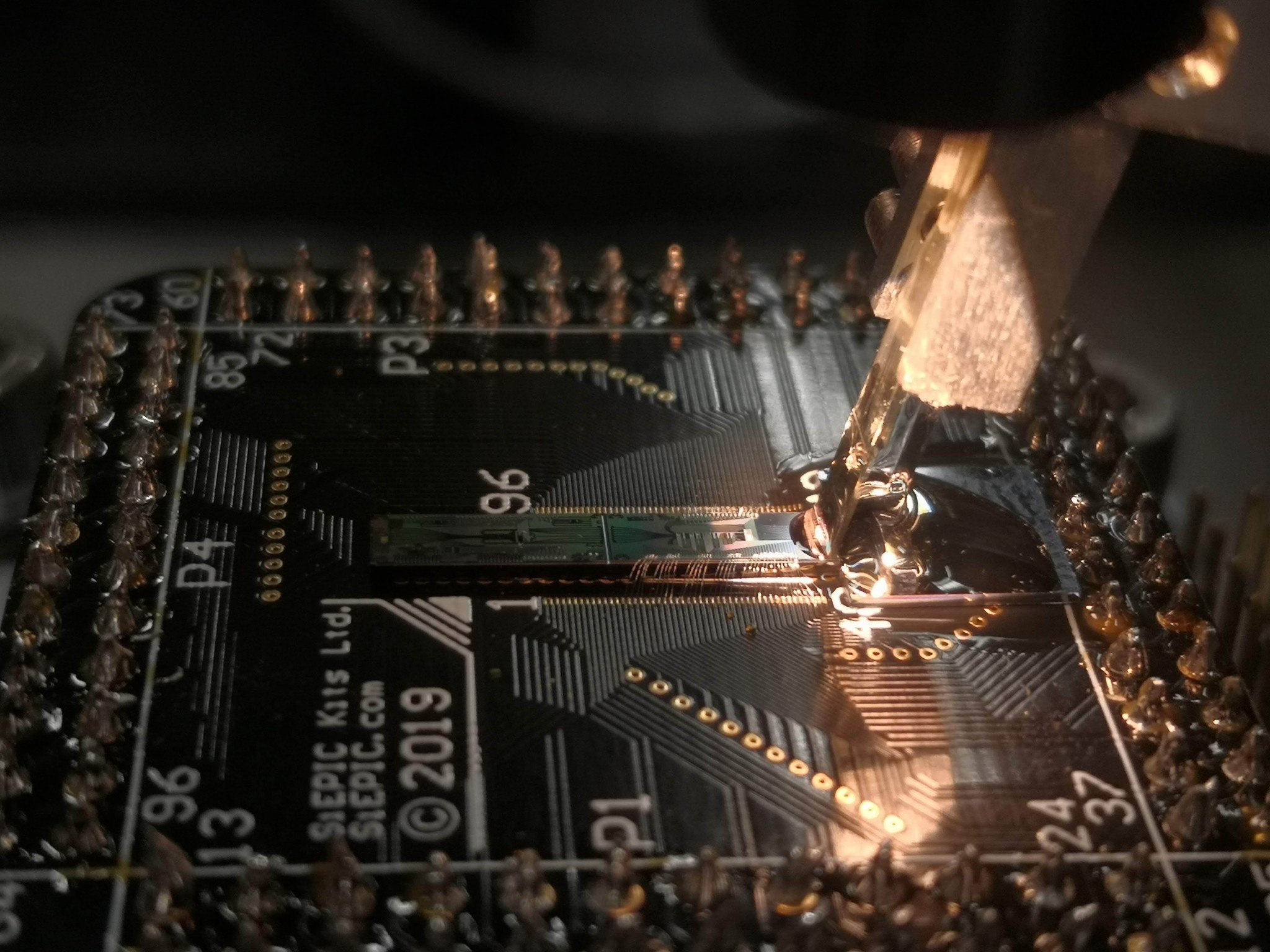
Testing and validation through member SiEPICkits. Automated PiC probe stations available through member Maple Leaf Photonics. Wafer-scale testing and automation through member EHVA
Silicon Photonics research is moving at an unprecedented pace -- accelerate your research and development by joining Canada’s SiP rapid prototyping consortium. Stay ahead of latest developments with access to bleeding edge processes. Collaborate with other members of Canada’s SiP Foundry.
Exposure to the entire silicon photonics ecosystem;
Access to pre-commercial fabrication processes
Regular early-access, member-only, process development and MPW runs
Rapid turnaround design, fabricate, test cycle
Access to unique fabrication tools, eg. photonic wire-bonding, EBL tool
Recruitment opportunities with research students and postdocs
Opportunities to participate in online and in-person workshops, courses, seminars and conferences
